


The human identity is made up of some really fascinating traits, and yet it still hasn’t known a trait bigger than our desire to improve under all circumstances. This desire, in particular, has enabled the …
0
The human identity is made up of some really fascinating traits, and yet it still hasn’t known a trait bigger than our desire to improve under all circumstances. This desire, in particular, has enabled the world to clock some huge milestones, with technology emerging as quite a major member of the group. The reason why we hold technology in such a high regard is, by and large, predicated upon its skill-set, which guided us towards a reality that nobody could have ever imagined otherwise. Nevertheless, if we look beyond the surface for one hot second, it will become abundantly clear how the whole runner was also very much inspired from the way we applied those skills across a real world environment. The latter component, in fact, did a lot to give the creation a spectrum-wide presence, and as a result, initiated a full-blown tech revolution. Of course, the next thing this revolution did was to scale up the human experience through some outright unique avenues, but even after achieving a feat so notable, technology will somehow continue to bring forth the right goods. The same has turned more and more evident in recent times, and assuming one new discovery ends up with the desired impact, it will only put that trend on a higher pedestal moving forward.
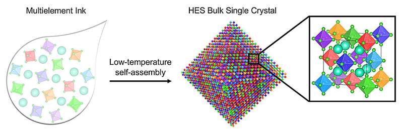
The researching teams at Lawrence Berkeley National Laboratory and UC Berkeley have successfully developed a new semiconducting material called “multielement ink”, which if found workable in reality, can make the process of semiconductor manufacturing significantly less heat-intensive. You see, the traditional approach to conducting the stated process demands a significant amount of heat-intensive energy, translating to scorching temperatures of around 2,700 degrees Fahrenheit. Furthermore, the subsequent purifying and assembling procedures would make the matters even more complicated, considering they can take weeks or even months at a time before they reach anywhere meaningful. But how does the new technology solve such a conundrum? Well, understood to be the first “high-entropy” semiconductor that can be processed at low-temperature or room temperature, the technology in question leverages two unique families of semiconducting materials: hard alloys made of high-entropy semiconductors; and a soft, flexible material made of crystalline halide perovskites. Talk about high-entropy materials, they are solids made of five or more different chemical elements that self-assemble in near-equal proportions into a single system. Now, even though these conventional high-entropy alloy materials require far less energy than silicon to process for manufacturing, they still cannot thrive without very high temperatures of over 1000 degrees Celsius (or over 1832 degrees Fahrenheit), a limitation which has kept the world from harnessing its potential so far. Fortunately enough, the team here would overcome the problem by banking upon the unique qualities of a well-studied solar material named halide perovskites. In case you didn’t know, perovskites can be easily processed from solution at low temperature, with its range stretching across room temperature to around 300 degrees Fahrenheit. So, basically, the researchers used the low energy requirement to synthesize high-entropy halide persovskite single crystals from a solution under room temperature or low-temperature (80 degrees Celsius or 176 degrees Fahrenheit) conditions. Going by the available details, the initial tests indicated that the resulting octahedral and cuboctahedral crystals were indeed high-entropy halide perovskite single crystals. As for the time exhausted, the low-temperature/room-temperature technique can produce single-crystal semiconductors within hours of mixing a solution and precipitating, significantly faster than conventional semiconductor fabrication techniques.
“Intuitively, making these semiconductors is like stacking octahedral-shaped molecular ‘LEGOs’ into larger octahedral single crystals. Imagining each of these individual molecular LEGOs will emit at different wavelengths, one can in principle design a semiconductor material that would emit an arbitrary color by selecting different molecular octahedral LEGOs,” said Peidong Yang, the senior author of the study.
Another limitation that the new technology overcame talked to stability issues usually encountered at ambient temperatures, and it did so by showcasing an impressive ambient-air stability of at least six months.
When quizzed regarding the possible use cases for such a system, the researching team hinted at its value around something like a color-tunable LED or other solid-state lighting device, or as a thermoelectric for waste heat recovery. Also, the technology can serve as a programmable component in an optical computing device that uses light to transfer or store data.
“Our high-entropy halide-perovskite semiconductor crystals, with their room-temperature and low-temperature methods, can be incorporated into an electronic device without destroying the other necessary layers, thus allowing for easier design of electronic devices and for more widespread use of high-entropy materials in electronic devices,” said Maria Folgueras, co-first author of the study and a former graduate student fellow in the Peidong Yang group at Berkeley Lab and UC Berkeley.