


There is a lot that came together to spell human progression in the way it actually occurred, and yet nothing here contributed more than our ability of improving at a consistent pace. We say this …
0
There is a lot that came together to spell human progression in the way it actually occurred, and yet nothing here contributed more than our ability of improving at a consistent pace. We say this because the stated ability has brought the world some huge milestones, with technology emerging as quite a major member of the group. The reason why we hold technology in such a high regard is, by and large, predicated upon its skill-set, which guided us towards a reality that nobody could have ever imagined otherwise. Nevertheless, if we look beyond the surface for one hot second, it will become clear how the whole runner was also very much inspired from the way we applied those skills across a real world environment. The latter component, in fact, did a lot to give the creation a spectrum-wide presence, and as a result, initiated a full-blown tech revolution. Of course, the next thing this revolution did was to scale up the human experience through some outright unique avenues, but even after achieving a feat so notable, technology will somehow continue to bring forth the right goods. The same has turned more and more evident in recent times, and assuming one new discovery ends up with the desired impact, it will only put that trend on a higher pedestal moving forward.
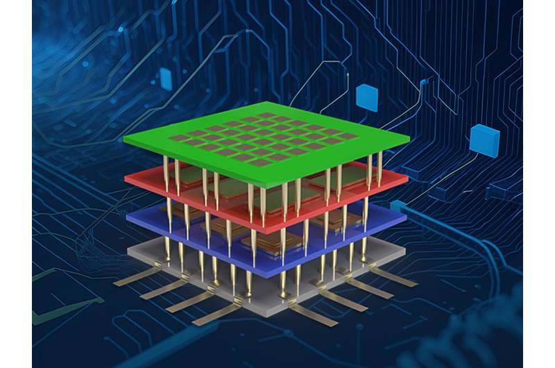
The researching team at Pennsylvania State University has successfully developed a technique to solve the limitations faced by Moore’s law, and therefore advance the field of electronics. To give you some context, Moore’s law is a fundamental scaling principle for electronic devices that expects number of transistors on a chip to effectively double after every two years. Now, while we have seen a rather meteoric progression in this area, we now stand at a point of saturation. You see, with today’s most advanced chips holding nearly 50 billion transistors, it has become an enormous challenge to store more of them, thus putting the Moore’s law on a rather tricky ground. Talk about how Pennsylvania State University’s researchers solved the stated conundrum, they proposed a solution in the form of 3D integration. Simply speaking, the semiconductor industry comprehends 3D integration as a process where you stack multiple layers of semiconductor devices in a vertical form. By doing so, one can conceive a concept called “More Moore”, where a bigger package of silicon-based transistors is placed upon a computer chip. Furthermore, the mechanism also allows the use of transistors made from 2D materials to incorporate diverse functionalities within various layers of the stack, translating to concept usually known as “More than Moore.”
“Monolithic 3D integration offers the highest density of vertical connections as it does not rely on bonding of two pre-patterned chips—which would require microbumps where two chips are bonded together—so you have more space to make connections,” said Najam Sakib, graduate research assistant in engineering science and mechanics and co-author of the study.
Having said so, monolithic 3D integration comes with its own set of limitations. For instance, it has been repeatedly discovered that conventional silicon components can easily melt under the processing temperatures.
“One challenge is the process temperature ceiling of 450 degrees Celsius (C) for back-end integration for silicon-based chips—our monolithic 3D integration approach drops that temperate significantly to less than 200 C,” said Darsith Jayachandran, graduate research assistant in engineering science and mechanics and co-corresponding author of the study, explaining that the process temperature ceiling is the maximum temperature allowed before damaging the prefabricated structures. “Incompatible process temperature budgets make monolithic 3D integration challenging with silicon chips, but 2D materials can withstand temperatures needed for the process.”
Fair enough, in their response to the given problem, the researchers marked a major first by using 2D transistors to do the job. These transistors were, on their part, made from 2D semiconductors called transition metal dichalcogenides. Moving on, one more detail we must mention here is how vertically stacking the devices in 3D integration also ensured a more energy-efficient computing, as it was able to solve a longstanding problem of distance among these transistors.
“By stacking devices vertically on top of each other, you’re decreasing the distance between devices, and therefore, you’re decreasing the lag and also the power consumption,” said Rahul Pendurthi, graduate research assistant in engineering science and mechanics and co-corresponding author of the study.
From an overall standpoint, we can say that the decreased distance between transistors enabled the integration of more elements, eventually making up a successful representation of “More Moore.” Coming back to the representation of “More than Moore”, it revealed itself, as we know, after 2D materials were introduced to the mix, materials that brought their unique electronic and optical properties, including sensitivity to light. The 2D component in this whole picture also delivered a benefit in the form of superior carrier mobility, which refers to how an electrical charge is carried in semiconductor materials. Hold on, there is more. The material’s ultra-thin size was what further freed up the space for researchers to fit more transistors on each tier of the 3D integration, leading them up to significantly more computing power.
With technological prowess covered, we now must turn our attention towards the development’s value at an industrial level. This should depict that, while most academic research has shown to involve small-scale prototypes, the current study oversaw 3D integration at a big scale, characterizing tens of thousands of devices. But how did it get there? The answer again includes those high-quality, wafer-scale transition metal dichalcogenides developed by researchers at Penn State’s Two-Dimensional Crystal Consortium (2DCC-MIP), a U.S. National Science Foundation (NSF) Materials Innovation Platform and national user facility.
“This breakthrough demonstrates yet again the essential role of materials research as the foundation of the semiconductor industry and U.S. competitiveness,” said Charles Ying, program director for NSF’s Materials Innovation Platform. “Years of effort by Penn State’s Two-Dimensional Crystal Consortium to improve the quality and size of 2D materials have made it possible to achieve 3D integration of semiconductors at a size that can be transformative for electronics.”